Views: 235 Author: Dongguan PRES Publish Time: 2026-08-06 Origin: Site


Content Menu
● Why PEEK Is the Material of Choice for Plasma Etch Insulators
● Dongguan PRES Group: Your PEEK Supply Partner for Semiconductor OEMs
● Thermal and Chemical Stability: What It Means in Real Etch Tools
>> Thermal Stability Under Process Conditions
>> Chemical Stability in Aggressive Plasma Environments
● Selecting the Right PEEK Grade for Plasma Etch Insulators
>> Machined Parts vs. Molded vs. 3D‑Printed
● Practical Steps to Improve Insulator Performance and Lifetime
● Industry Context: Where PEEK Fits Among High‑Performance Polymers
● Why Buyers Choose Dongguan PRES Group for PEEK Insulators
● Call to Action: Optimize Your Plasma Etch Insulators with PRES
● FAQ
PEEK insulators for plasma etching equipment combine thermal and chemical stability to deliver reliable dielectric performance in aggressive semiconductor environments. At Dongguan PRES Group Co., Ltd., we engineer and supply high‑purity PEEK grades—pellets, sheets, rods, tubes, powders, and 3D printing filaments—tailored for OEMs building plasma etch tools that run hotter, cleaner, and longer.

Plasma etching (RIE, ICP, DRIE) exposes components to high‑energy plasma, reactive fluorine/chlorine species, elevated temperatures, and hard vacuum. Insulators must maintain dimensional stability, resist chemical attack, and provide consistent electrical isolation under these conditions.
PEEK (polyetheretherketone) meets these demands with a unique balance of properties:
- Continuous service temperature up to ~260°C, with short‑term tolerance beyond that
- High melting point (~343°C) and glass transition around 143°C, enabling stable performance across wide thermal cycles
- Low outgassing under vacuum, minimizing particle generation and contamination risk
- Excellent chemical resistance to acids, bases, and many solvents—critical in fluorine‑rich etch chemistries
- Strong dielectric strength and stable insulation under combined thermal/electrical stress
Compared to metals, PEEK eliminates metallic contamination; compared to many polymers, it resists thermal degradation and hydrolysis, making it ideal for insulating spacers, standoffs, bushings, and chamber liners in plasma equipment.
As a China‑based high‑performance plastics manufacturer, Dongguan PRES Group focuses on PEEK, PPS, PEI, PPSU, PES, PSU, PAI, PI, and related engineering polymers. We support foreign brand owners, distributors, and equipment manufacturers with OEM/ODM production of semi‑finished and finished PEEK parts.
Our core capabilities for plasma etch applications include:
- PEEK pellets and granules for injection molding and extrusion of insulator components
- PEEK sheets, rods, tubes, and profiles for machining custom spacers, rings, and fixtures
- PEEK powders for specialized coatings and composite formulations
- High‑performance 3D printing filaments for rapid prototyping of complex insulator geometries
- Custom compounding (e.g., glass‑ or carbon‑filled PEEK) to tune stiffness, wear resistance, and ESD behavior
We work closely with customers to align material grade selection, tolerance control, and traceability with semiconductor equipment requirements.
In plasma etch chambers, temperatures can fluctuate rapidly during process ramps, cleaning cycles, and maintenance. PEEK's semi‑crystalline structure gives it a sharp melting point rather than a broad softening range, reducing the risk of gradual thermal deformation.
Key thermal benefits for insulators:
- Stable dimensions across repeated thermal cycles, preserving critical gaps and alignment
- Low thermal expansion and creep resistance, maintaining clamp forces and spacing over time
- Low thermal conductivity (≈0.24–0.26 W/m·K), which helps electrically isolate hot zones while limiting heat transfer to sensitive sub‑assemblies
Etch processes use fluorine‑ and chlorine‑based gases (e.g., CF₄, Cl₂, HBr) that can attack many polymers and elastomers. PEEK's aromatic backbone and strong intermolecular forces provide:
- Resistance to hydrolysis and steam, even after prolonged exposure
- Inertness to most acids, bases, and hydrocarbons, except concentrated sulfuric acid
- Low moisture absorption (~0.2%), limiting swelling and property shifts in humid or wet‑clean environments
This chemical robustness translates into longer service life, fewer unscheduled maintenance events, and more consistent process performance.
Not all PEEK is identical. Grade selection depends on mechanical load, temperature profile, contamination limits, and electrical requirements.
- Unfilled PEEK: Best for maximum chemical resistance, toughness, and dielectric performance. Ideal for general insulators and low‑load spacers.
- Glass‑filled PEEK: Higher stiffness and dimensional stability; useful where tight tolerances and reduced creep are critical.
- Carbon‑filled or ESD‑safe PEEK: Provides controlled surface resistivity to prevent electrostatic discharge while retaining much of PEEK's thermal and chemical performance—valuable near sensitive wafer handling zones.
- Machined from sheet/rod/tube: Preferred for low‑to‑mid volumes, complex geometries, and tight tolerances. PRES supplies semi‑finished PEEK profiles optimized for CNC machining.
- Injection‑molded: Best for high‑volume insulator components with consistent geometry. We supply PEEK pellets and can support mold development and process optimization.
- 3D‑printed PEEK: Enables rapid iteration of insulator designs, internal channels, and lightweight structures. Our high‑temperature 3D printing filaments support functional prototypes and some end‑use parts.
To maximize the value of PEEK insulators in plasma etch equipment, consider the following engineering practices:
1. Define the thermal envelope clearly
Map peak temperatures, dwell times, and cycle counts. Ensure the selected PEEK grade's continuous service temperature exceeds your worst‑case process window with margin.
2. Control contamination from the start
Specify low‑outgassing grades and clean processing. Use PEEK's natural low particle generation to your advantage in front‑end modules where yield is critical.
3. Design for mechanical stability
Use appropriate wall thicknesses, ribbing, and support features to minimize stress concentrations. Leverage PEEK's creep resistance, but avoid over‑loading thin sections in high‑temperature zones.
4. Account for chemical exposure patterns
Identify which surfaces face direct plasma and which see only background gases. In extremely aggressive zones, consider hybrid designs (e.g., PEEK insulator with localized ceramic or polyimide shielding) while keeping PEEK as the primary structural dielectric.
5. Validate with real‑world testing
Run thermal cycling, vacuum outgassing, and chemical exposure tests that mirror your actual process recipes. Use the data to refine tolerances, surface finishes, and maintenance intervals.
While polyimide remains the go‑to for the very highest temperature plasma zones (>300°C continuous), PEEK offers a highly attractive balance for many insulator applications where temperatures stay within its range and where chemical resistance, mechanical strength, and cost‑effective manufacturability are paramount.
Typical semiconductor components made from PEEK include:
- Wafer handling fingers and end‑effectors
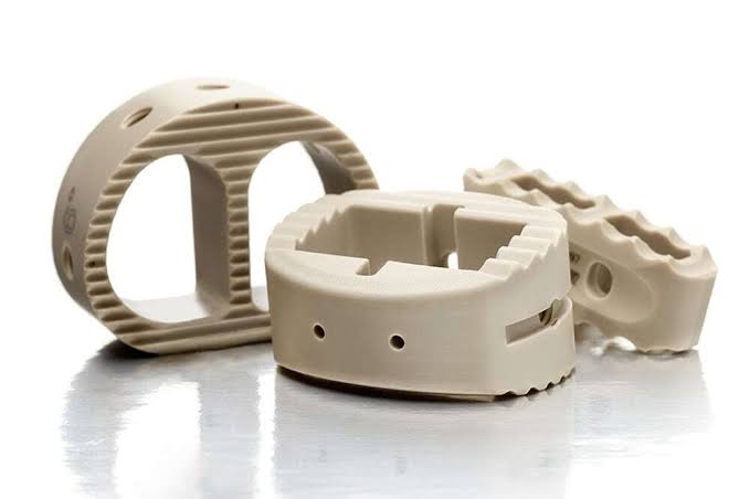
- Insulating spacers and standoffs in plasma chambers
- Precision bushings and valve seats
- Structural parts in inspection and metrology systems
For many OEMs, PEEK insulators deliver longer run times between maintenance, reduced contamination risk, and simplified supply chains compared with mixed metal/ceramic solutions.
Customers working with Dongguan PRES Group highlight several differentiators:
- One‑stop PEEK supply: From pellets to finished parts, we cover the full value chain for plasma equipment OEMs.
- Technical collaboration: We help translate process requirements into material specs, tolerances, and inspection plans.
- Flexible manufacturing: Small‑batch machined parts, pilot runs, and scaled production with consistent quality.
- Global OEM support: We regularly serve foreign brand owners, distributors, and equipment manufacturers with OEM/ODM programs.
For teams developing or upgrading plasma etch tools, partnering early with a PEEK specialist can shorten development cycles and reduce total cost of ownership.
If you are designing or refurbishing plasma etching equipment, and you need PEEK insulators that deliver thermal and chemical stability without compromising electrical performance, Dongguan PRES Group is ready to support your project.
- Request PEEK grade recommendations for your specific etch process
- Discuss custom profiles, machined parts, or 3D‑printed prototypes
- Explore OEM/ODM cooperation for long‑term supply
Contact our engineering team to review your application and define a PEEK solution that improves uptime, yield, and maintainability.
1. Mitsubishi Chemical Advanced Materials – "PEEK plastics – Polyetheretherketone properties & applications"
https://www.mcam.com/en/products/peek
2. Dongguan Pres Plastic Materials Co., Ltd. – Company and product overview (Made‑in‑China)
https://dgpres.en.made-in-china.com/
3. Craftech Industries – "PEEK in Semiconductor Manufacturing"
https://craftechind.com/peek-in-semiconductor-manufacturing/
4. Fluorotec – "High‑Performance Polymers in Semiconductor Equipment"
https://www.fluorotec.com/news/blog/high-performance-polymers-semiconductor-equipment/
5. SpecialChem – "Polyetheretherketone (PEEK): How to select the right grade?"
https://www.specialchem.com/plastics/guide/polyetheretherketone-peek-thermoplastic
6. AON3D – "PEEK Material Properties and Applications"
https://www.aon3d.com/material-science/peek-material-properties-and-applications/
7. Polyfluoro Ltd. – "High‑Performance Polymer Components for the Semiconductor Industry"
https://polyfluoroltd.com/blog/high-performance-polymer-components-for-the-semiconductor-industry-peek-pps-and-polyimide/
8. Dongguan Pres Plastic Materials – PEEK parts and glass‑filled PEEK rod listings
https://dgpres.en.made-in-china.com/product-group/MqLTwAbuXDhz/PEEK-parts-1.html
https://peek-materials.sell.everychina.com/
9. Coorstek – "Ceramic Components for Plasma Etch Equipment" (industry context)
https://www.coorstek.com/en/industries/semiconductor/etch/
Q1: What makes PEEK suitable for insulators in plasma etching equipment?
A1: PEEK combines high continuous service temperature (~260°C), excellent chemical resistance to aggressive etch gases, low outgassing under vacuum, and strong dielectric properties—making it ideal for insulating spacers, standoffs, and chamber components in plasma etch tools. [mcam]
Q2: How does PEEK compare to polyimide for plasma etch applications?
A2: Polyimide tolerates higher continuous temperatures (>300°C) and is preferred for the hottest plasma zones, while PEEK offers superior chemical resistance, mechanical toughness, and easier manufacturability for many insulator applications where temperatures remain within PEEK's range. [fluorotec]
Q3: Can Dongguan PRES Group supply custom‑machined PEEK insulators?
A3: Yes. We provide PEEK sheets, rods, tubes, and profiles optimized for CNC machining, and can produce custom insulators, spacers, and fixtures to your drawings and tolerances as part of OEM/ODM programs. [dgpres.en.made-in-china]
Q4: Are there ESD‑safe or conductive PEEK options for semiconductor equipment?
A4: Yes. Carbon‑filled or specially compounded ESD‑safe PEEK grades provide controlled surface resistivity to prevent electrostatic discharge while retaining much of PEEK's thermal and chemical stability, useful near sensitive wafer handling areas. [fluorotec]
Q5: How do I start a PEEK insulator project with PRES?
A5: Share your process conditions (temperature, gases, vacuum level), mechanical loads, and electrical requirements. Our team will recommend a PEEK grade, propose a manufacturing route (machined, molded, or 3D‑printed), and outline a development and supply plan. [dgpres.en.made-in-china]
Hot Tags: China, Global, OEM, private label, manufacturers, factory, suppliers, manufacturing company